Published
by Rogers Corporation
Advanced Electronics Solutions
As electronic devices continue to shrink in size and increase in power, demand grows for power electronic circuits with higher power density. Increased operating temperatures are one of the tradeoffs of higher circuit power density, resulting in an increase in thermal stress for the circuit materials that serve as substrates for modern power electronic circuits. New processes and materials are available to address these challenges.
Soldering vs Silver Sintering
Soldering can present a number of complications that reduce a circuit’s performance, such as solder bridges and heel cracking. At higher operating temperatures, solder fatigue becomes an issue. Common die attach technologies are based on soft solders with melting points below 250°C. With the development of new generations of semiconductors (e.g. based on wide band gap materials like SiC and GaN), operating temperatures increase to more than 200°C. This will lead to a significant decrease in the solders‘ strength and reliability.
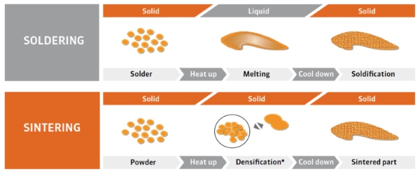
Sintering is a heat treatment process applied to a powdered material in order to give it higher strength and integrity. Silver sintering has become a promising technology for high temperature power electronics packaging as an alternative to soldering.
In the soldering process, heat is applied until a solid reaches its melting point and is then allowed to cool down and solidify to form a bond. In the silver sintering process, heat is applied to a silver paste, resulting in densification. Several actions occur simultaneously, including grain growth, pore growth, and densification, resulting in a stronger bond.
Find out what you need to know about silver sintering in the tech note: curamik® Substrates for Silver Sintering.
PCB Materials for High Power, High Temp Applications
The requirements for PCB materials capable of supporting high-density power electronics circuits are quite challenging, since they include both mechanical and electrical stability at high temperatures.
To meet these demands, curamik® ADVANTAGE provides a ceramic-materials based solution for smaller, higher power-density PCB circuits in power electronic applications. These ceramic substrates provide low dielectric loss and low-loss copper conductors that support high voltages and currents in power-grid, energy, and industrial power applications.
To improve the performance and usability of the substrate materials, all curamik ADVANTAGE products include a choice of plating materials, addition of solder stop to control solder coverage, and treatment for surface roughness. As an alternative to soldering, a state-of-the-art silver sintering process provides an attachment option to solder for critical high-temperature applications
Download the Power Magazine article for more details: Tailoring Circuit Materials for Power Electronic Applications
Watch the curamik ADVANTAGE video:
Published on Jul 25, 2017