Published
by Olivier Mathieu, Market Development Manager
Advanced Electronics Solutions
In a recent Olivier’s Twist blog, the topic of Silicon Carbide semiconductor materials was discussed for future high power efficiency applications. There is also another semiconductor technology that is filling a gap in performance between Silicon and Silicon Carbide, and that is Gallium Nitride.
What are some advantages of GaN devices?
GaN is what is also considered a “wide bandgap” material. As noted in the previous blog, “The band gap generally refers to the energy difference in electron volts (eV) between the valence band and the conduction band.” Materials with band gaps between 2-4 eV are typically thought of as being wide bandgap semiconductors. However, there are some exceptions to this rule with Gallium oxide (-Ga2O3), Diamond, and Aluminum Nitride (AlN1).
When we take a look at a table comparing Silicon to Silicon Carbide to Gallium Nitride, it starts to become clear where some of the trade-offs are between the two wide bandgap semiconductors.
| Properties | Si | SiC | GaN |
| Energy Gap (eV) | 1.12 | 3.26 | 3.4 |
| Breakdown Field (MV/cm) | 0.3 | 3 | 3.5 |
| Thermal Conductivity (W/mK) | 150 | 490 | 130 |
| Electron Drift Velocity (cm/s)x107 | 1 | 2.7 | 2.5 |
| Electron Mobility (cm2/V-sec) | 1450 | 900 | 2000 |
Table 1: Some common properties of Silicon, Silicon Carbide, and Gallium Nitride
Gallium Nitride and Silicon Carbide both have similar bandgap energies, breakdown fields, and electron drift velocities. This also means that they both are capable of higher power densities when compared to Silicon enabling significantly smaller devices. However, GaN has an electron mobility twice as high as SiC and 25% higher than Si. While the electron drift velocity dictates average velocity that electrons move through a semiconductor when and electric field is applied across the material, the electron mobility describes the ease at which electrons can move in an electric field. This property coupled with GaN’s lower losses at high frequencies means that GaN devices can obtain higher switching frequencies than either Si or SiC. The electron mobility of GaN is also what makes it very attractive for HEMTs (High Electron Mobility Transistors) for applications in microwave communications and RF technology.
In the field of RF and microwave communications, GaN is also ideal for satellite communications due to its resistance to ionizing radiation. The high electron mobility of GaN (when used in HEMTs mentioned above) makes it possible for better power amplification in satellite frequency bands for satellite communications uplink (frequencies listed below). Current research into this material has indicated that, by reducing the size of the GaN on SiC chip, expanded communications band frequencies can go beyond 30 GHz allowing for more complex data to be transmitted to satellites.
| Spectrum Band | Communication Frequency |
| X-Band | 7.9-8.4 GHz |
| Ku-Band | 13.75-14.5 GHZ |
| Ka-Band | 29-31 GHz |
Table 2: Common satellite frequencies for satellite communications uplink.
A single-chip MMIC (Monolithic microwave integrated circuit) can produce an output power of more than 60W in the X-band and 20 W in the Ka-band2. The current semiconductor used in satellite communications, GaAs (Gallium Arsenide), is larger, heavier, and has a lower output power, so GaN semiconductors can capitalize on its 8X better raw power density and 70% efficiency increase to replace these GaAs semiconductors for improved satellite performance. The high heat resistance of SiC make it ideal for electronics in high heat applications (solar satellites and planetary sensors), so SiC (also resistant to ionizing radiation) is also being used for advanced satellite applications.
What is the difference between GaN and SiC?
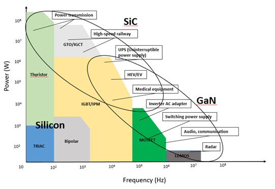
The high switching frequency of GaN semiconductors make it a good candidate for other applications like radar technology and high switching power supplies such as those for data centers. The high thermal conductivity of SiC semiconductors make it ideal for things like power transmission, high-speed transportation, and more efficient renewable energy. Generally speaking, GaN is limited to around 650V power applications, while SiC is good for applications above 1.2kV (additionally, GaN’s switching losses are more than 3X lower than SiC at 650V). There are some applications where the two overlap, so the more established or inexpensive technology may win out in these markets. The below graphic is a good representation of the difference between these two markets and how they compare to the current Silicon market.
Figure 1: Comparison of markets for Silicon, SiC, and GaN.
What are the disadvantages of GaN?
Perhaps one of the biggest disadvantages to GaN compared to SiC is the manufacturing process. GaN has historically been grown on wafers for use in blue diode lasers, so generally speaking, the available wafers are smaller than SiC. Additionally, SiC can be grown homoepitaxially (it is grown on a substrate of the same material), where GaN is grown on either Si or SiC wafers. This can lead to lower yield of GaN devices and also accounts for the Thermal Conductivity of GaN devices being well below the theoretical value of 330-540 W/mK.
Since GaN is heteroepitaxial, the crystals cannot be used for “vertical devices” which means that there is a need for bigger chip sizes and additional topside contacts compared to SiC architectures. Generally speaking, vertical devices are better for the amount of voltage and current that they can control. However, compared to SiC, GaN devices semiconductors can be grown faster with multiple chips to a substrate, and the Si substrate-based GaN devices are becoming increasingly better quality.
There are two different camps for the future of wide bandgap semiconductors, GaN and SiC. Both technologies have niche applications with wider applications currently favoring SiC. Bringing the cost and time of manufacturing down will be critical in determining which technology gains more of a foothold in new markets like EV/HEV. Additionally, development of a reliable method to obtain a homoepitaxial GaN semiconductor will be paramount in order for GaN to be used more widely.
The compact size and higher power capabilities of GaN semiconductors mean they have a higher heat density that will need to be managed in order to run efficiently. Rogers offers a number of heat sink and liquid cooling options and the Power Electronics Solutions team is happy to assist with design questions.
1- “PowerAmerica Strategic Roadmap for Next Generation Wide Bandgap Power Electronics”, PowerAmerica, Version 1.0, February 2018
2- “GaN Empowers Satellite Communication”, Mike Coffey, Steve Richeson, and Michael DeLisie from Mission Microwave, Compound Semiconductor Vol. 24 Issue 7, Oct. 19, 2018
Related Products:
ROLINX Busbars
Tags:
General Industrial, Rail, Wind & Solar
Published on May 25, 2019