Published
by Pablo Paz Sagues, Development Engineer
Advanced Electronics Solutions
Stray inductance of switching circuits is one of the most critical parameters in the design of power electronics and is becoming even more important for systems using wide-bandgap semiconductors, such as SiC and GaN.
The operating principle of power electronics is based in switches (the semiconductor devices) commutating at frequencies in the order of kHz to create low frequency or DC power. When a switch changes its state, it must deal with the voltage and current in the circuit. For example, in the case of ON to OFF switching, current flowing in the switch tends to continue flowing which can be regarded as an electric inertia or inductance. When this current reaches the closed switch it “crashes” into it like a wave into a breakwater wall, creating a spike in voltage. Thus, the higher the inductance the higher the voltage surge in the semiconductors. In fact, this phenomenon is analogue to a water hammer where the speed of liquid flowing in a pipe transforms into an overpressure when we close the tap (that is why any plumber would advise to always close the taps gently).
There are other negative effects linked to the inductance of power circuits, such as EMI (electromagnetic interference). For a given current, a high inductance is a consequence of high unrestrained magnetic flux and can be reduced by correctly routing and shaping the conductors.
Here is where laminated busbars come into play: the inductance of a conductor depends on its shape, the proximity of the current paths and the lowest inductance geometry given by parallel planes: exactly the structure of a busbar. When required to reduce inductance to a minimum, the laminated busbar brings conductors extremely close to each other, in some cases under 100µm.
The inductance of a pair of wires 1 mm apart and 1m in length is around 0.4 mH. It may seem to be a low value but for power electronics the required inductance is in the range of the nano Henries. The equivalent construction in a busbar of the same section would be 50 nH which is already 88% lower. Additionally, if the distance between conductors is reduced by a high-end insulation, for example 0.2mm, inductance is reduced to below 20 nH.
This was an ideal case to show the potential of busbar construction and the calculations that can be performed using simple formulas. In real application, the shape of a busbar is much more complex and must comply with many other requirements such as connection points (to semiconductor devices, to capacitors, to power cables or other busbars), insulation for the required voltage level, adequate thermal dissipation, fixation elements, and of course manufacturability.
Inductance measurement of real busbars has traditionally been performed by a lab or field testing. It requires highly specialized equipment and a delicate set up. Additionally, at least one prototype must be manufactured. The effect of small changes in the geometry of the busbar can have a large impact on the inductance, therefore it is extremely difficult to build a sample that can be modified for testing and optimization. However, Finite Element Method simulations do not require a physical sample and modifications can be easily done in the 3D model of the busbar. This allows a fast-iterative process that translates into a very low inductance solution. Furthermore, other features of the busbar can be evaluated in parallel by FEM simulations such as current distribution and thermal behavior which leads to a highly optimized busbar. When a busbar is simulated to evaluate its inductance a plot of the magnetic field is obtained. As mentioned before, the inductance is proportional to the magnetic field. Besides, a simulation allows a fast sweep along a wide range of frequencies, reaching up to MHz. This is especially valuable as magnetic flux is highly dependent on the frequency and each system is designed for a particular switching frequency and slope. Consequently, due to the simulation results it is easy to pin-point the most critical areas for improvement and act on them.
In the following paragraph, it will be demonstrated how a typical inductance optimization is performed.
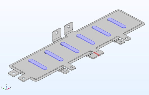
The first step is to 3D model the busbar that shall be simulated. Typically, semiconductor devices and capacitors are not included in the model. The capacitors are substituted by a short-circuit that allows current to flow following the lowest-impedance path. In order to calculate this path simulation software considers all electromagnetic physics constrains, including proximity and skin effect at high frequencies. In the connection of the semiconductor devices the probe to evaluate the inductance is placed.
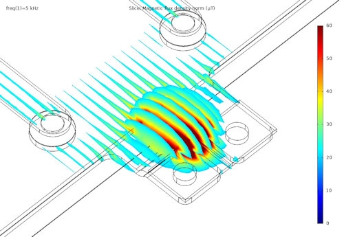
The next image shows the 3D model of the first busbar design. The elements highlighted in blue are the short-circuit blocks at the capacitor positions and the red element is the probe which is placed at the connection of the central IGBT in this case.
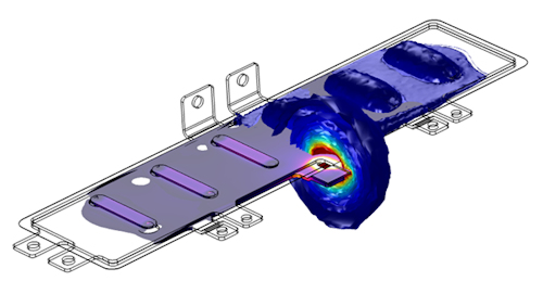
The simulation shows the areas in and around the busbar with a high magnetic flux (values in µT, as probe current is only 1 A). It can be observed that the highest magnetic flux, thus the largest contribution to the inductance is found in the connection terminal of the IGBT. The second largest contributors are the capacitor connections.
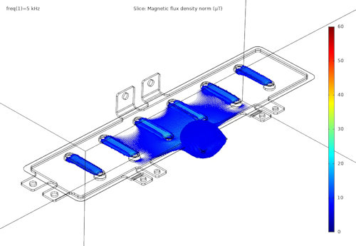
The total inductance of this system at the simulation frequency of 5kHz is 12.0 nH.
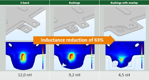
When zooming into the terminal area it is noted that the magnetic flux is created in the open loop between the terminals. Thus, why it is highly recommended to optimize this part to have a large impact in the inductance reduction.
The first optimization consists in changing the bend terminal from the original design into a flat terminal with connection bushings. This allows to reduce the open gap and decreases the inductance to 9.2 nH.
In a second optimization loop the overlap between the terminals is increased, which reduces the flux in the area. As a result, the inductance is further reduced to 4.5 nH.
The optimization could continue and tackle other areas of the busbar, but it has been demonstrated that with a fast approach the inductance of the original part has been reduced by 63% to a value below 5 nH. With the right tools, knowledge and experience FEM simulation is an ideal approach to optimize the inductance of a laminated busbar (which is, by construction, the lowest inductance structure) in order to boost the performance of any power electronics system.
Do you have any question or require some information about our busbars or simulations? Please contact us, if you need assistance.
Related Products:
ROLINX Busbars
Tags:
Automotive & EV/HEV, General Industrial
Published on Jan 12, 2021