Published
by Olivier Mathieu, Market Development Manager
Advanced Electronics Solutions
The copper grain size is an important property of Direct Bonded Copper (DBC) substrates. Variations in the copper grain size cannot be fully excluded, but large variations may affect the subsequent assembly processes or the performance of DBC substrates. Module manufacturers can rely on the experience and competence of Rogers' Power Electronics Solutions (PES) team to deliver substrates with a consistent grain size. In this blog, we explain why variations in copper grain size should be limited and what Rogers' PES team is doing to limit such variations.
Influence of copper grain size on assembly process and substrate performance
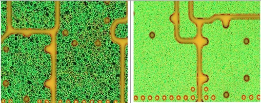
Module makers use camera systems and automated optical inspection systems during their assembly process. Those systems rely on the reflection of light to accurately place components on the substrate or detect failures. However, the reflection of light depends on the copper grain size. A fine-grained copper surface has diffused reflection properties, meaning there is a homogeneous reflection of light on the surface. On the contrary, the reflection direction on a coarse-grained copper surface differs depending on each copper grain. The pictures below show a typical difference in the reflection of light from a coarse-grained copper surface on the left side and from a fine-grained copper surface on the right side. Process engineers can usually optimize their machine settings to handle one or the other grain size but cannot tolerate large variations in grain size from batch to batch or within one production batch.
In addition, the copper grain size has an impact on the substrate´s warpage and lifetime. Thermal cycling investigations have shown that degradations appear first on DBC substrates with fine copper grain size. Crystalline imperfections known as dislocations can easily move throughout the crystalline grains but grain boundaries stop dislocations. Smaller grains have a greater ratio of surface area to volume, which means a greater ratio of grain boundary to dislocations. The more grain boundaries exist, the higher the strength becomes. Consequently, copper with a fine grain size is less deformed during thermal cycling, meaning the ceramic is exposed to more thermo-mechanical stress and ultimately cracks earlier than with coarse-grained copper.
Therefore, it is not surprising that module makers are asking their DBC substrates suppliers to control the copper grain size and limit grain size variations from batch to batch and between the front and back side. However, this requires good knowledge of the direct copper bonding process and raw copper material.
Factors that affect the copper grain size
The copper grain size of DBC substrates depends on the raw copper material itself, as well as the direct copper bonding process.
For the direct copper bonding process, it is mandatory to use high-grade, oxygen-free copper with standardized designation Cu-OFE and material number CW009A; which has been developed specifically for electronic and heat transfer applications. It is extremely pure with a maximum oxygen content of 5ppm (0,0005%). Next to the oxygen content, impurity elements and their concentrations in raw copper material are critical parameters for the direct copper bonding process. At Rogers, we have installed specifications with the suppliers of raw copper material. All copper shipments carry a test certificate which guarantees that impurities in the material are below the specified limits. Though the total content of impurities is less than 50ppm (0,0050%) with no single impurity exceeding 25ppm (0,0025%), variations in the chemical composition cannot be excluded. This may lead to copper grain size variations after the bonding process.
However, the suppliers of raw copper material cannot guarantee the copper grain size of the DBC substrates. The direct copper bonding process, especially its temperature profile, has a significant influence on the copper grain size of the finished goods. As a consequence, the copper grain size should be measured after the bonding process.
Measurement method of copper grain size and typical values
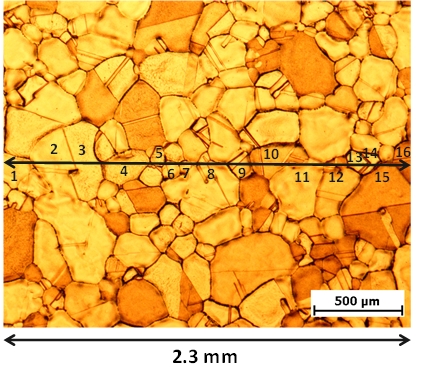
At Rogers, each raw copper coil is inspected. A sheet of copper is taken from the coil. It is then oxidized and bonded with the ceramic. Finally, the substrate is cleaned in order to remove copper oxide from the surface before the copper grain size can be measured. Usually, an optical microscope is used to measure the copper grain size. The copper grain size is defined as the number of grains per mm. Typical values vary between less than 3 grains per mm (coarse-grained copper) up to more than 10 grains per mm (fine-grained copper).
For example, the picture below shows 16 grains along a line with 2.3mm length. This means that the copper grain size along this line is 2.3mm / 16 = 144µm or 16 / 2.3mm = 7.0 grains / mm. The same measurement is repeated on 5 parallel lines and 5 perpendicular lines to calculate an average value.
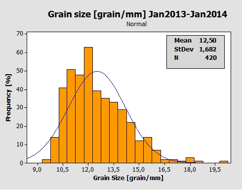
For almost four decades, the Rogers' PES team has been producing DBC substrates. We have delivered billions of substrates to the power electronics and automotive industries. Over the years, we have gained a lot of experience and have continuously improved our direct copper bonding process to provide the best trade-off between state-of-the-art assembly processes and substrate performance to achieve a consistent quality. In 2013, a study was conducted to understand the copper grain size and its variation. The histogram below shows the distribution of the average copper grain size of DBC substrates during the study´s period.
As assembly technologies evolve and module makers need to improve substrates´ performance, copper grain size may have to be further optimized. At any rate, consistent quality is required and the Rogers PES' team has the knowledge and competence to adapt to your needs. Do you have any question or require some support with the design and selection of a suitable substrate for your application? Please contact us, if you need assistance.
The information herein is for reference only. Neither the author nor Rogers makes any warranties as to its contents.
Related Products:
curamik Ceramic Substrates
Tags:
Aerospace & Defense, General Industrial, Major Appliances, Rail, Wind & Solar
Published on Apr 06, 2020